Photonics, Plasmonics and Teratronics
Photonic and plasmonic circuits exploit fundamental principles of light-matter interaction to enable novel signal processing concepts at unprecedented speed and energy efficiency.
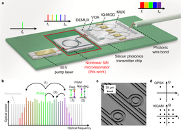
Our research covers both technologies and applications of nanophotonic devices. On the technology side, the focus is on design, fabrication and characterization of silicon photonic circuits and plasmonic devices, using a combination of external foundry services and in-house fabrication in our state-of-the-art cleanroom facilities. On the application side, we investigate teratronic signal processing concepts for handling of Tbit/s data streams and of signals with THz bandwidths.

Nanophotonics employs fundamental opto-electronic principles of light-matter interaction to implement novel functionalities on chip scale at lowest footprint, lowest energy consumption and highest operating speed. The focus is on design, fabrication and characterization of Silicon Photonic and Plasmonic devices in our state-of-the-art cleanroom facilities and characterization laboratories.

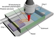
Photonic wire bonds fabricated by 3D lithography enable the seamless combination of various photonic integration platforms, for e.g., to realize high-speed energy-efficient transceivers. This new fabrication technology enables low loss interconnects with a high density without the need for active alignment.

The goal of this interdisciplinary research group is to develop photonic sensor systems for applications in chemistry, biology, and the life-sciences. The developed sensors are based on active and passive microoptical cavities, which are integrated on a chip with microfluidic structures.
Bio-Inspired Photonics (H. Hölscher)
Biophotonic Sensors (C. Koos)

The Teratronic Signal Processing Group specializes in pushing the technological limits of the on-chip signal processing into the Tbit/s regime using high-speed plasmonic modulators and detectors which exploit the high non-linearity and fast response of electro-optic polymers.

